Noise Muting FM Receiver
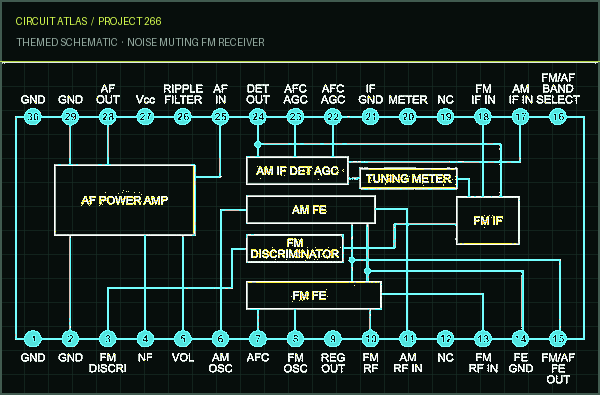
Fig. 1: Functional block diagram of Sony CXA1619S When a frequency modulated (FM) receiver is tuned to an FM radio station's frequency, there is a lot of "hissing" noise in between the st…
Know the mission before touching a wire.
Understand what you are making, prepare the right tools, and make the workbench safe.
Project details
Noise Muting FM Receiver is a electronics project. Fig. 1: Functional block diagram of Sony CXA1619S When a frequency modulated (FM) receiver is tuned to an FM radio station's frequency, there is a lot of "hissing" noise in between the st…
- Source pages
- 508-512
- Named parts
- 5
- Build goal
- Working, tested prototype
Tools you need
- Digital multimeter
- Wire stripper and side cutters
- Soldering iron with a fine tip
- Current-limited bench supply
Use eye protection, good lighting, and a clean insulated surface throughout the build.
Safety precautions
- Disconnect every power source before changing a connection.
- Check component polarity, pinout, and supply voltage twice.
- Use a current limit for the first power-up.
- This project may involve hazardous voltage. Work only with qualified supervision and proper isolation.
Gather, identify, and understand every part.
Use the standardized inventory, then open What's this? to learn each part's role, advantages, limitations, handling, and specifications.
What's this?Image, role, pros, cons, handling & specifications
Power supply
A power component supplies, converts, stores, or regulates energy for the project.
What it does hereIt must provide the documented voltage, polarity, isolation, and sufficient current safely.
Buy / compare this part ↗Advantages
- Stable power improves reliability
- Current limiting protects first tests
- Regulation reduces resets and noise
Limitations
- Wrong polarity can cause immediate damage
- Underrated parts overheat
- Mains circuits require qualified supervision
Handling
- Measure output before connection
- Use a fuse or current limit
- Insulate exposed conductors
Specifications to verify
- Use the exact model, value, package, and rating listed for Power supply; similar-looking parts are not always interchangeable.
- Confirm input/output voltage, current, polarity, connector, isolation, and thermal rating.
What's this?Image, role, pros, cons, handling & specifications
 SEMICONDUCTOR LEARNING VIEW
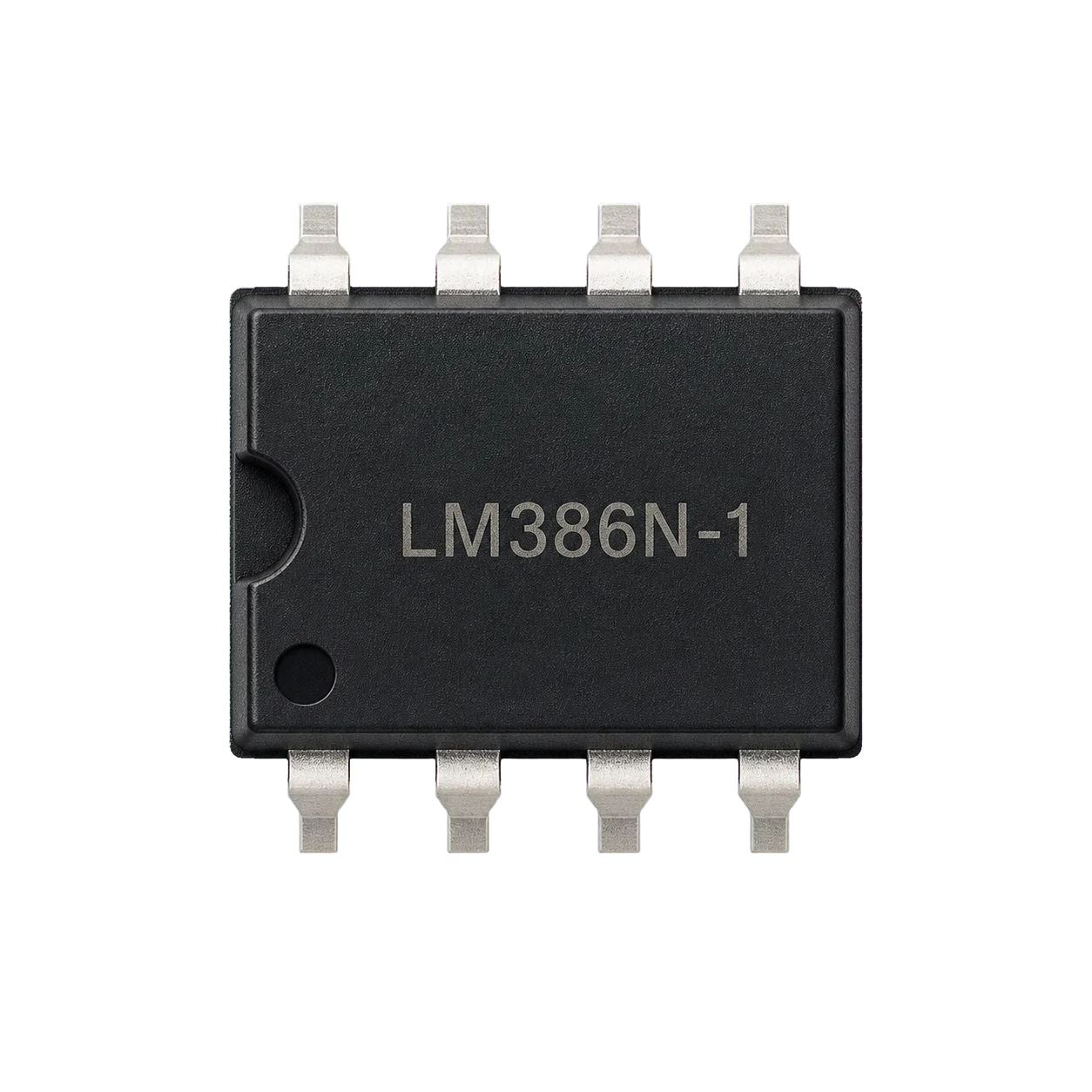
LM386
A semiconductor stage performs switching, amplification, regulation, rectification, or logic.
What it does hereIt controls current or signal flow at a defined point in the circuit.
Buy / compare this part ↗Advantages
- Fast and efficient
- Compact
- Can control larger loads from smaller signals
Limitations
- Pin order varies
- Sensitive to overvoltage and reverse polarity
- May need cooling or bias components
Handling
- Verify the datasheet pinout
- Avoid static and soldering heat
- Check notch, stripe, or flat-face orientation
Specifications to verify
- Use the exact model, value, package, and rating listed for LM386; similar-looking parts are not always interchangeable.
- Confirm pinout, maximum voltage/current, dissipation, gain or forward voltage, and package.
What's this?Image, role, pros, cons, handling & specifications
CD40106
A semiconductor stage performs switching, amplification, regulation, rectification, or logic.
What it does hereIt controls current or signal flow at a defined point in the circuit.
Buy / compare this part ↗Advantages
- Fast and efficient
- Compact
- Can control larger loads from smaller signals
Limitations
- Pin order varies
- Sensitive to overvoltage and reverse polarity
- May need cooling or bias components
Handling
- Verify the datasheet pinout
- Avoid static and soldering heat
- Check notch, stripe, or flat-face orientation
Specifications to verify
- Use the exact model, value, package, and rating listed for CD40106; similar-looking parts are not always interchangeable.
- Confirm pinout, maximum voltage/current, dissipation, gain or forward voltage, and package.
What's this?Image, role, pros, cons, handling & specifications
 SEMICONDUCTOR LEARNING VIEW
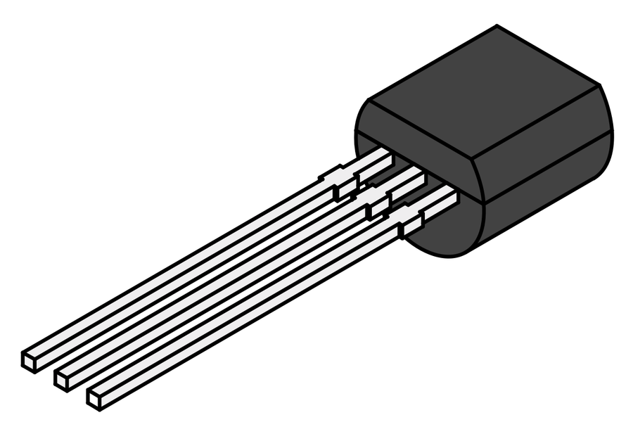
BC548
A semiconductor stage performs switching, amplification, regulation, rectification, or logic.
What it does hereIt controls current or signal flow at a defined point in the circuit.
Buy / compare this part ↗Advantages
- Fast and efficient
- Compact
- Can control larger loads from smaller signals
Limitations
- Pin order varies
- Sensitive to overvoltage and reverse polarity
- May need cooling or bias components
Handling
- Verify the datasheet pinout
- Avoid static and soldering heat
- Check notch, stripe, or flat-face orientation
Specifications to verify
- Use the exact model, value, package, and rating listed for BC548; similar-looking parts are not always interchangeable.
- Confirm pinout, maximum voltage/current, dissipation, gain or forward voltage, and package.
What's this?Image, role, pros, cons, handling & specifications
T1 - transistor stage identified in the circuit
A semiconductor stage performs switching, amplification, regulation, rectification, or logic.
What it does hereIt controls current or signal flow at a defined point in the circuit.
Buy / compare this part ↗Advantages
- Fast and efficient
- Compact
- Can control larger loads from smaller signals
Limitations
- Pin order varies
- Sensitive to overvoltage and reverse polarity
- May need cooling or bias components
Handling
- Verify the datasheet pinout
- Avoid static and soldering heat
- Check notch, stripe, or flat-face orientation
Specifications to verify
- Use the exact model, value, package, and rating listed for T1 - transistor stage identified in the circuit; similar-looking parts are not always interchangeable.
- Confirm pinout, maximum voltage/current, dissipation, gain or forward voltage, and package.
Connect one verified path at a time.
Explore the named components and standardized signal flow, then use Source Check to verify exact physical pins, values, and topology before applying power.
Trace this circuit.
Noise Muting FM Receiver: interactive parts, standardized terminals, responsive anchored wires, student explanations, and the original circuit reference in one shared system.
Trace before wiring
Follow power, ground, inputs, processing, and outputs in that order. Never guess a pin from package shape alone.
Connect with power off
Make short, labelled connections and share a common ground only where the schematic requires it.
Inspect every joint
Check continuity, polarity, adjacent shorts, and loose connections before the first power-up.
Open all source diagrams and build views 3 visuals
Confirm the hardware-only control path.
This project does not include firmware in the source. The circuit itself provides the required behaviour.
How to connect
- Match every controller label to the circuit view and source pin map.
- Join grounds before signal wires when separate low-voltage supplies are used.
- Keep motors, relays, pumps, and other loads on a suitable driver and external supply.
Common mistakes
Reversed VCC/GND, board-label versus GPIO-number confusion, missing common ground, and charge-only USB cables.
Troubleshoot
Disconnect loads, continuity-test one path at a time, then test with a current limit.
Software preparation
No IDE, board package, library, or firmware upload is required for this project.
If you add a programmable controller as an extension, document its pin map separately.
How to upload code
The original design is implemented entirely in hardware, so proceed after verifying the circuit and supply.
Assemble, deploy, test, and troubleshoot.
Use the complete source notes in build order, then pass the final checks before calling the project finished.
Build in functional stages
- Power and regulation
- Controller or processing stage
- Inputs and sensors
- Outputs and loads
- Enclosure and strain relief
Power up safely
- Inspect unpowered continuity first
- Apply the lowest safe current limit
- Measure supply rails before signals
- Add one load at a time
- Record expected and actual results
Work from simple to complex
- Confirm power, ground, polarity, and orientation
- Compare each pin with the source
- Test inputs separately from outputs
- Replace only one variable at a time
- Power off before every correction
Follow the documented instructions.
These notes come from this project's source and remain in their original order.
Project overview
Project build noteFig. 1: Functional block diagram of Sony CXA1619S When a frequency modulated (FM) receiver is tuned to an FM radio station's frequency, there is a lot of "hissing" noise in between the stations, which is very annoying for the operator and, therefore, not a good thing. Digital FM receivers don't have this problem because the output is automatically cut off when there are gaps between stations. Digital FM receivers, on the other hand, are much more expensive than their analogue counterparts.
Analog FM receivers use an LC tuning system that makes "hiss" noise at the output. This noise doesn't get cut off when the receiver is tuned off- station. But if the received signal level is good (i.e., if the receiver frequency is close to that of an FM station), the limiter circuit that comes before the ratio detector circuit in an analog FM receiver will cut off any noise that is riding the FM carrier. The simple noise-muting FM receiver circuit described here stops this "hissing" noise from coming out of the output of an analog FM receiver circuit when it is not tuned to the frequency of an FM station. In other words, when the tuner circuit of an analog FM receiver is switching between FM stations, this circuit mutes the output of the receiver.
Circuit Description
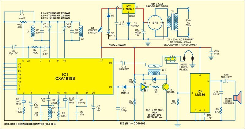
Project build noteThe circuit for the noise-muting FM receiver is built around a Sony CXA1619S AM/FM receiver chip, which comes in a 30-pin PDIP package. Sony FM receiver chips are known for having better features and being more affordable. Fig. 1 shows a block diagram of how the chip works. Fig. 3 shows the whole circuit of the FM receiver, including the power supply and the circuit that mutes the sound. Most FM kits on the market also use the Sony CXA1619S, which is an AM/FM receiver IC that doesn't need many extra parts. It can work with as little as 3V of power. Here, we've used a 6V supply so that we can connect the receiver's output directly to a 32-ohm headphone or a low-power AF amplifier built around IC LM386. A 3-pin jumper is there to let you choose what you want. The tuning meter output at pin 20 of the CXA1619S is used by the circuit that mutes the sound. Fig. 2 shows the chip's internal circuit around pin 20. Usually, a light-emitting diode is used to show that the tuning is correct (LED). The cathode of the tuning indicator LED is connected to pin 20, and
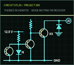
the anode is connected to the positive supply through a current-limiting resistor. Fig. 2: Internal circuit schematic around pin 20 of CXA1619S When the receiver is tuned to the center of the FM carrier, pin 20 of the CXA1619 goes very low and the LED lights up the brightest. Circuit connections Diode D1 was used to connect pin 20 of the CXA1619S to the input of a CMOS inverter gate instead of an LED. In the "off" tuning condition, when the receiver is not tuned to any FM station, input pin 1 of CMOS inverter gate N1 (1/6 CD40106) is biased to 2/Vcc using a potmeter arrangement made up of resistors R6 (33 kilo-ohms) and R7 (68 kilo-ohms). So, between FM stations, the output pin 2 of the inverter gate stays low, so transistor T1 (BC548) stays off and the 5V inverter relay connected to its collector stays off. But when an FM station is selected, the receiver's output pin 20 and the input pin 1 of the CMOS inverter gate both go low. So, the output of the inverter gate goes high, which makes transistor T1 turn on the relay.
Fig. 3: Complete circuit of the noise muting FM receiver including the power supply The audio output from the CXA1619S, which is available at pin 28, is sent to either the headphones or the AF amplifier circuit via the 100F capacitor C12 and the contacts of the reed relay. This happens when the relay is energized, which only happens when the receiver is tuned to the carrier frequency of an FM station. So, the annoying noise the receiver makes when it is tuned to a "off" station doesn't come out of the headphones or the loudspeaker. In other words, the noise is muted when the receiver is not tuned to an FM station because of the way the circuit is set up around the CMOS inverter gate. Power supply The output of IC 7806 is used to power the inverter gate N1 (IC3), transistor T1, and FM receiver chip/kit. This keeps the voltage in the whole circuit at a constant level. If the mains power goes out or if the device needs to be portable, four 1.5V cells can be used instead. Diode D3 in the power supply circuit makes sure that the battery output is not used when the mains power is on.
Antenna You can use either a 75cm telescopic antenna or a wire of the same length as an antenna. Circuit operation When there is no FM station being picked up, diode D1 doesn't conduct, so pin 1 of inverter gate N1 stays high and pin 2 of the inverter stays low. So, transistor T1 doesn't work, and relay RL1 stays off. So, whether the load is a headphone or an audio power amplifier stage driving a loudspeaker, as shown in Fig. 3, no sound will come out of the headphones or loudspeaker. In other words, the CXA1619S doesn't play sound when the receiver isn't tuned to an FM station's frequency.
You built Noise Muting FM Receiver.
You followed the full workflow from understanding the mission to testing the finished project. That is a real engineering achievement - well done.
PC Based Stepper Motor Controller
Ready to reuse what you learned in another project from the same track?
Start this project →